Explain photovoltaic effect. With required diagrams discuss construction and working of solar cell.
Photovoltaic effect: “The effect due to which light energy is converted into electrical energy is called photovoltaic effect.” It was first discovered by Edmund Becquerel in 1839.
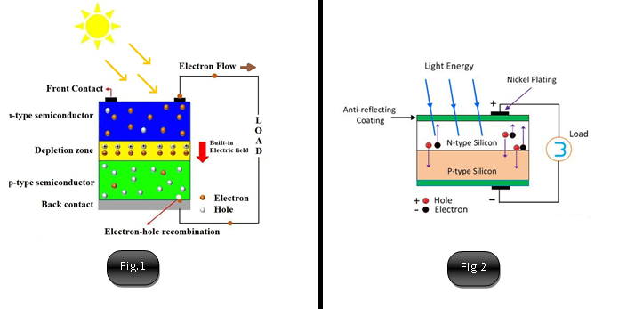
- The photovoltaic effect occurs in solar cells that are composed of two different types of semiconductors, p-type and n-type joined together to form a p-n junction.
- Whenever these semiconductors are joined, an electric field is formed in the region as electrons move to p-side and holes move to n-side.
- This movement of electron creates an electron hole pair so, free electrons from n-type region try to diffuse to p-type region and holes in p-type region try to diffuse to n-type region in the crystal.
- Each free electron of n-type region while comes to the p-type region due to diffusion, it leaves a positive donor ion behind it in the n-type region.
- These positive and negative ions concentration layer creates an electric field across the junction which is directed from positive to negative that in from n-type side to p-type side.
- Due to this electric field (E) electrons experience a drift in the direction of field and generates drift current.
- So, diffusion of charge carriers creates and increases the thickness of the potential barrier across the junction and drift of the charge carriers reduces the thickness of the barrier.
- In normal thermal equilibrium condition, the diffusion of charge carrier is equal and opposite of drift of charge carriers, hence the thickness of potential barrier remains fixed.
- Now the n-type surface of the silicon crystal is exposed to the sunlight. So, when light of suitable wavelength is incident on these cells, energy from the photons is transferred to the semiconducting materials in the p-n junction. This energy causes electrons to jump to a higher energy level (conduction band), leaving behind a hole in the valence band.
- So, it is this movement of electrons creates an electron hole pair, leading to a flow of current in the cell.
Construction of solar cell:
- P-N junction is one of the essential requirement in the construction of solar cell.
- This P-N junction is constructed by using semiconducting materials such as germanium silicon, gallium arsenide, cadmium arsenide, etc.
- The P-N junction is packed in a cylindrical metal container with a glass window on top so that light may fall on both P-and N-type materials uniformly.
- In order to avoid recombination of generated electrons in the P-and N-regions, their thickness is kept very small.
- For the generation of more number of charge carriers under the influence of incidenting light, heavily doped P-and N-type of materials are used.
- Thus, the use of heavily doped P-and N-regions gives a large photo voltage.
- Nickel plated metal ring around P-type layer act as the positive output terminal and the metal contact at the bottom serves as the negative output terminal.
Working of solar cell:
- When the photons of suitable energy allowed to incident on P-N junction, photons impart sufficient energy to the valence electrons and remove them from their parent atoms.
- Hence, electron-hole pairs are generated in both P-region and N-region of the junction (as shown in Figure).
- These newly generated charge carriers reach the depletion region by diffusion where they are separated by a strong potential barrier existing there.
- At the same time, the minority charge carriers (electrons in P-region, holes in N-region) are supported by the existing potential barrier at the junction for their flow across the junction.
- Flow of minority charge carriers across the junction constitute the minority current, which is directly proportional to the illumination and also depends on the surface area being exposed to the light.